Memory is one of the important subsystems in a Computer. It is a volatile storage system that stores Instructions and Data. Unless the program gets loaded in memory in executable form, the CPU cannot execute it. CPU Interacts closely with memory for execution.
There are many other storage systems in a computer that share the characteristics with memory. So why have so many storage systems? Everyone desires to have very large, super fast and cheap storage. Storage cost varies depending on the type of storage. Memory devices are hierarchically connected to design a cost-effective memory. When we say memory, we refer to the main memory, commonly referred to as RAM.
Memory (Storage Device) Characteristics
Although Memory and Storage devices share many a characteristic, there is uniqueness in each one of them. Some of the most important characteristics are as below:
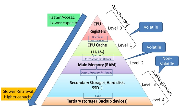
- Access Time - The access time depends on the physical nature of the storage medium and the access mechanisms used. Refer to figure 17.1. At the bottom is access time in Milliseconds, while at the top of the triangle it is less than 10 ns.
For memory, the access time can be calculated as the time difference between the request to the memory and service by memory.
- Access Mode - Access mode is a function of both memory organization and the inherent characteristics of the storage technology of the device. Access mode has relevance to the access time. There are three types of access methods.
- Random Access: If storage locations can be accessed in any order then access time is independent of the storage location being accessed. Ex: Semiconductor memory.
- Serial Access: Memory whose storage locations can be accessed only in a certain predetermined sequence. Ex: Magnetic tape
- Semi Random: The access is partly random and there apart serial. Ex: Hard disk, CD drives. It is random to locate the tracks and access within the track is serial.
- Retention - This is the characteristic of memory relating to the availability of written data for reading at a later time. Retention is a very important characteristic in the design of a system.

- Cycle Time - Is defined as the minimum time between two consecutive access operations. This is greater than the access time. Generally, when once access is over, there is a time gap required to start the next access, although minimal. Cycle time = Access time + defined time delay. Ex: You ask the shop keeper of what is the speed of the memory strip.
- Capacity - Measured in Units of Bytes, Kilobytes, Megabytes, Gigabytes, Terabytes, Petabytes. In figure 17.1, the bottom of the triangle has a larger capacity and the ones at the top have the far lesser capacity. Ex: the Memory strip as 2GB, 4GB, Hard disk as 1TB, GPRs are 128 words.
- Cost Per bit – Factors of cost per bit are Access time, Cycle time, Storage capacity, the purchase cost of the device and the hardware to use the device (controller). We don’t have much choice on this; designers care for this.
- Reliability – It is related to the lifetime of the device. Measured as Mean Time Between Failure (MTBF), in the units of days/years. Ex: Think of how frequently you replace your Hard disk while the CPU is still usable.
Memory Hierarchy
There is a capacity/performance/price gap between each pair of adjacent levels of storage types (Refer figure 17.1). The objective of multilevel memory organisation is to achieve a good trade-off between cost, storage capacity and performance for the memory system as a whole.
Multilevel hierarchical memory is based on the principle of Locality of Reference i.e. the address generated by a program tend to be localised to successive address locations and therefore predictable. In figure 17.1, the unit of data movement between successive levels is also inscribed.
CPU Memory Interface
Level 0 to Level 3 of the storage devices are volatile memory subsystems which are accessed by CPU directly. The Level 4 and level 5 are storage devices which are classified as I/O devices and will be dealt with later as a separate category. So let us see about the CPU Memory Interface basics.
The CPU interacts with memory for two operations i.e READ or WRITE. READ is for getting either instructions or Data (Operands). Write is generally for writing results upon instruction execution. To access memory, the address of the memory location is required. This address is always loaded in the Memory Address Register (MAR) by the CPU. READ or WRITE operation is always carried out on the location specified by MAR. In the case of READ, the memory returns the data to the CPU while in the case of WRITE the data to be written onto the memory location is given by CPU. The data exchange happens via the Memory Data Register (MDR). The CPU communicates to the memory about the READ or WRITE activity as control signals. Also, some more signals to time the validity of information on the Address bus and Data bus are part of Control Signals.
The communication about the address and data and the associated Control signals happen in the bus. A bus is a set of physical connections between two entities used for communication using electrical signals. This external bus has three components namely,(i) Address bus, (ii) Data bus and (iii) Control Signals. Memory Address Register (MAR) and the Memory Data Register (MDR) play an important role in communication. The control signals are generated by the Control Unit. For more clarity refer to figure 17.2.
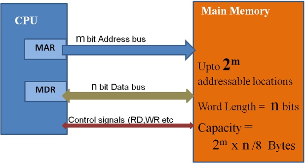
Please note that the address bus is unidirectional and the data bus is bidirectional for obvious reasons discussed above. The control bus is also bidirectional. Further, the width of the address bus and data bus have critical meaning. The CPU can READ or WRITE data equal to the width of the data bus in one access. Generally, the width of the data bus equals the CPU word width. The width or the number of bits in the address bus has a bearing on the maximum number of locations that can be addressed or accessed by CPU. The signals on the bus are synchronised with the CPU clock.
Data transfer rate or bandwidth is one of the measures of the performance of the external bus between CPU and Memory. The maximum amount of information that can be transferred to or from the memory per unit time is the data transfer rate or bandwidth and is measured in bits or words per second.
Memory Capacity Integration
Memory is often available in standard capacity strips or modules. More often we need to integrate these modules to meet our requirement. When more than a strip is assembled, how do the expansion and chaos-free access happen is a curiosity. We will see now.
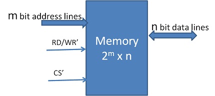
A typical memory module has the interface as shown in figure 17.3. This is in line with the signals on the external bus. A mention is required on RD/WR' and CS'. RD/WR' is a signal for READ or WRITE operation in mutual exclusion. When the signal is logical HIGH it is READ operation and when Logical LOW, WRITE is enabled on the Memory Module. CS' is Chip Select and active LOW i.e when this signal is logical LOW, only then the module is enabled and any operation can be done on this module. This Chip Select signal is useful in memory expansion. When RD is active, DataOUT comes from the module, while WR’ is active the direction of data is DATA-IN.
Memory expansion to the desired capacity is achieved by two means:
- Increasing the word width by a factor (Refer figure 17.4)
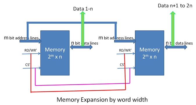
Figure 17.4 Memory expansion by word width - Increasing the Number of Words ( address) by a Factor ( Refer figure 17.5)

Figure 17.5 Memory expansion by address range
When the capacity is expanded to increase the addressable range, the CS' signal plays a role in selecting the correct block. The MSB bit(s) of the address is(are) decoded and connected to each module as CS' enable.In figure 17.5, a simple inverter (NOT logic) is used on the MSB line as there are only 2 modules. If there are more modules then a decoder is required. This kind of extrapolation is feasible to any capacity in multiples of the basic module.
Fast RAM Interfaces
The most important issue in design is to bridge the gap between CPU and Memory in terms of speed gap despite technological advancements. One option for speed enhancement is Cache Memory design at Level 1. Capacity expansion can be achieved by Virtual memory implementation at level 4. However, more is required for faster access and response from Main Memory. Modern-day memory modules are designed as variants of DDR technology. Double Data Rate per clock cycle is known as DDR. It is a design technique to increase the data transfer rate between memory and CPU. Following statements highlight the scenario of faster RAM access technologies.
| Single Data Rate Synchronous DRAM SDR SDRAM | 1 word of data per clock cycle |
|---|---|
| Double Data Rate Synchronous DRAM DDR SDRAM | 2 words per clock cycle |
| DDR2 SDRAM | 4 consecutive words per clock cycle |
| DDR3 SDRAM | 8 consecutive words per clock cycle |
| DDR4 SDRAM | 16 consecutive words per clock cycle |
| DDR5 SDRAM | 32 consecutive words per clock cycle |
The goal of every memory system is to provide adequate storage capacity with an acceptable level of performance and cost. This goal is achieved by employing several memory types in a hierarchical model.
