DMA is Direct Memory Access. As the name implies, DMA facilitates data transfer between I/O and Memory directly, instead of involving CPU as in the other two cases of I/O data transfer. DMA is faster and bulk data transfer technique. The system bus is common between CPU, Memory, DMA and maybe few I/O controllers. At an instant, the system bus can be used for communication between any two members only. Further, at a time, a resource can be used by only one entity. Thus when DMA communicates with Memory, the CPU will be on hold to use the System Bus. However, the CPU may do any other machine cycle internally using ALU and other resources. DMA Controller (DMAC) is special hardware which manages the above functions.
In Chapter 21, we have already discussed the overview of CPU, DMA coordination in achieving I/O data transfer.
DMAC operation
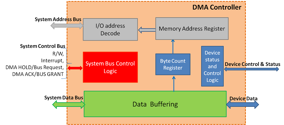
As you can see from figure 22.1, the DMAC is connected to the system bus. The I/O devices are connected to the DMA ports called Channels. A DMAC can generally support 4 I/O devices. The coordination between CPU and DMA happens with DMA raising DMA HOLD signal and the CPU responding with DMA HOLD ACK signal.

The sequence of events described below clarifies how an end to end data transfer happens between I/O device and Memory using DMA.
- CPU delegates the responsibility of data transfer to DMA by sending the following details:
- A device on which I/O to be carried out
- What is the command (R/W) to be carried out
- The starting address of Memory location for Data Transfer
- Length of the Data Transfer (Byte Count) - The first two information is given to the device controller while the last two information is stored in the channel register in DMAC.
- The I/O controller initiates the necessary actions with the device and requests DMAC when it is ready with data.
- DMAC raises the HOLD signal to CPU conveying its intention to take the System bus for data transfer.
- At the end of the current machine cycle, the CPU disengages itself from the system bus. Then, the CPU responds with a HOLD ACKNOWLEDGE signal to DMAC, indicating that the system bus is available for use.
- DMAC places the memory address on the address bus, the location at which data transfer is to take place.
- A read or write signal is then generated by the DMAC, and the I/O device either generates or latches the data. Then DMA transfers data to memory.
- A register is used as a byte count, decremented for each byte transferred to memory.
- Increment the memory address by the number of bytes transferred and generate new memory address for the next memory cycle.
- Upon the byte count reaches zero, the DMAC generates an Interrupt to CPU.
- As part of the Interrupt Service Routine, the CPU collects the status of Data transfer.
DMA to Memory Data Transfer Modes
The data transfer modes are about how does the CPU acquires the system bus for its activity. There are three options available in the DMAC, namely Cycle Stealing, Burst Mode and Hidden Mode.
Cycle Stealing: The DMAC steals the system bus (Memory cycles) from the CPU, during its non-memory machine cycles like Decode or execute, to transfer a byte/word to/from memory. Cycle stealing is possible when there is a separate arbitrator logic for the system bus. It is to be noted that, in the case of HOLD and HOLD ACK sequence, CPU acts as bus arbitrator. The DMAC steals the bus for every transaction, hence the name cycle stealing.
Burst Mode: Once the DMAC takes the bus, it completes the data transfer with the necessary number of cycles. Holds the system bus until the Byte Count reaches zero, after which it releases the bus. The CPU is halted during the data transfer. Since the intended block is transferred in one bus access, Burst mode is also called Block Transfer Mode. In this case, the DMAC is assigned an equal priority with CPU.
Transparent or Hidden Mode: There are some internal states during which the CPU frees the bus, disengaging itself. At these times, DMA takes up data transfers to memory. In this mode, the DMA is assigned the lowest priority, rather it never contends for the bus. The CPU speed is never affected by DMA. Not only DMA requires extra logic to detect the floating bus but also CPU requires extra logic to indicate its status. The throughput of DMA is poor and the data transfer is slowest of all the modes. Figure 22.2 explains when the CPU can recognise DMA or Interrupt. These points are called breakpoints.

DMA Controller Functional Components
It has all the functional components of any I/O controller. Since DMA communicates on the system bus, required additional logic is in-built. The bus control logic generates R/W signal and Interrupt. Depending on the DMA data transfer mode, bus arbitration signals are generated. The bus arbitration signals are DMAHOLD or Bus Request, DMA HOLD ACK or BUS GRANT as the case may be.

Byte Count Register is an important register which holds and tracks the byte transfer taking place with Memory. CPU sets the value. It is decremented for every byte transferred and the Memory address register is updated to show the next location for data transfer. When the byte count becomes zero, it indicates End of Data Transfer. This status is used for generating an interrupt signal to CPU.
Buffered Data Transfer takes place at the device end. The required control signals are generated. This part is very much similar to I/O Controller.
Generally, DMA has more than one channel to facilitate more I/O devices connection. In such a case, we will have duplicity of Memory Address Register, Data Buffer, Status and Control Registers and Byte Count register. The interface logics remain common.
Advantages of DMAC
- Certainly speeds up the data transfer to memory with minimal bus holding
- Relieves the CPU for its task
In the case of DMAC, the CPU is involved to initiate every single IO Operation. Although the DMA method is better than the Programmed IO and Interrupt driven IO, overall system performance can be improved if there is a design methodology which will take care of total I/O with simple initiation from CPU. The IO Processor (IOP) design supports this requirement.
I/O Processors
I/O processors (IOP) are an extension to the DMA concept of I/O Operation. As the name implies, I/O processors have some processing capacity for serving the device controllers connected to it. IOPs can decode and execute I/O instruction. These instructions are brought from Main Memory by the IOP. Data transfer happens with Memory directly. Thus an IOP has a fair amount of control over IO Operations with very minimal initiation from CPU.
IOPs are also called Peripheral Processing Unit (PPU). I/O Channels is a name used in Mainframe to mean IOP.

Characteristics of IOP
- Has Instruction set catered to IO operations
- It can execute a sequence of instructions called "I/O Program" on a device connected to it.
- Ability to decode and execute IO instructions for a variety of devices. Each device has unique commands that can be executed on them.
- DISK – RESET, SEEK, READ, WRITE, FORMAT, Error Checking, etc
- TAPE – REWIND, FORWARD, WRITE, READ, BOT, EOT, etc
- PRINTER – LINE FEED, FORM FEED, WRITE, PRINT, etc
- High-Speed Data transfer to increase the IO Performance
- Variety of devices can be connected
- Multiplexed IOP connects slow speed device controllers
- Selector IOP for high-speed device controllers
- Similar to DMA channels, IOP also has channels to connect Device controllers
- IOP is connected to System Bus
- Possible to have more than one IOP in a system configuration
Functioning of IOP
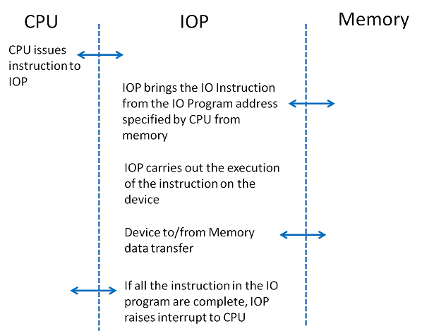
IOP frees CPU from I/O data transfer operations. The CPU is involved to the extent of informing the address of the I/O program in memory. And the IOP is expected to get the IO Program, decode and execute. After the data transfer is complete, the IOP raises an Interrupt to CPU. The communication steps between CPU, IOP and Memory in completing data transfer is depicted in figure 22.5

CPU – IOP Instruction
The instruction issued by CPU to IOP has three parts:
- CPU Opcode indicating that the instruction is to instruct IOP
- IO Device Address – it is the target device on which the IO program is to be executed
- IO Program Address – It is a Main Memory Address where the set of commands to be executed on the IO Device is stored.

From the third part, it is clear that the CPU does not get involved in instructing the IO devices. Corresponding to each IO Device, an IO Program is stored in Memory. The IO program consists of a set of instructions to be executed on the device notified by the CPU Instruction to IOP.
IO Program
A typical IO program is much like any other program, except that it has IO Instructions to be executed on a select device.

An I/O instruction received by IOP from memory as part of the IO Program has four parts as below:

- IO Opcode – the IO instruction to be executed on the device
- If it is a Data Transfer instruction, the memory address for data transfer. For data transfer, IOP accesses memory via the system bus. It contends on the bus based on the bus arbitration logic design.
- If it is a Data Transfer instruction, the size of the data transfer – Data transfer count
- Control information – how this instruction to be executed in terms off error handling, interrupts etc. and also, whether any more instructions are chained and hence follows this instruction. This is a very useful feature. IT has bits assigned to indicate End of IO Program
Any data transfer operation on DISK is preceeded by a SEEK command to position the heads on the place where the file is located. Command chaining helps.
Also if data transfer is to happen from more than one area of disk, chaining of SEEK + data transfer is done easily with IO program.
Many such examples in the case of printer, tape and other devices can be given.
For CPU it is too costly to get involved in these scenario. Thus, IOP improves the IO and CPU performance.
IOP Instruction Categories
The IOP is likely to receive the following categories of instructions.
- Data transfer instructions - for doing data transfer.
- Branch instructions - allow the IOP to fetch the next CCW form a specified memory location instead of from the contiguous location
- Arithmetic and logical instructions – facilitate the calculation of memory addresses, IO Device priorities and so on
- IO Device Control instructions - These are not data transfer ones; these are transmitted to the device and specify functions peculiar to that device. Ex: seek, rewind, Top of form etc.
We have seen the IOP fetching instructions from memory, decoding, controlling, calculating, etc. This is as much a mini CPU. It requires most of the functional logic of CPU like program counter, decoder, flags, etc. Thus the name IO Processor is justified.

