What is a datapath? Why a datapath?
Let us understand how do we do addition and what is required to carry out addition. Let us say we are solving the following problem.
"A class has 26 boys and 30 girl students. Find the total number of students?"
The micro and nano steps to realized are:
- Identify how many boys, how many girls
- Understand that the sum to be solved using addition
- In your notebook, on a new page, create a workspace
- In the workspace, write 26 in a line and 30 in another line
- Now do the addition, if required use rough space for work out
- Rewrite this as result = 56
Oh! you are a geek. Your computer also needs to do all these or more steps to solve this problem. In fact, in the process of solving the problem,
- the CPU has to get this instruction from memory
- know the address of the memory location wherein the data about boys and girls are kept
- decode the instruction to be ADD
- Get the boys girls data from memory to CPU workspace (Registers)
- Navigate this data to ALU so that addition can be carried out
- Write the result from ALU to the Result Space.
So, if we are using our brain and notepad space, the CPU uses Registers, ALU, MEMORY, etc. The functional components that make up the requirements of all the instruction execution. The DATAPTH is a collection of registers, ALUs, multiplexers, status registers and their interconnection are called DATAPATH.
A DATAPATH is the collection of state elements, computation elements, and interconnections that together provide a conduit for the flow and transformation of data in the processor during execution
The DATAPATH is unique to each CPU. It is designed to meet the ISA and performance of ISA. A DATAPATH is part of the microarchitecture. It is a low-level design specific implementation of the ISA. The DATAPATH is controlled by control unit i.e the timings and enabling the path is managed by the Control Unit. The DATAPATH is configured, designed and implemented only once for a CPU. The DATAPATH is not reconfigurable. Research is going on for feasibility of reconfigurable datapath.
Datapath Elements
Essentially a DATAPATH consists of the following elements.
ALU – one or more to carry out the computation. ALU is not only used in data operations but also in address calculation too.
Instruction Register and decoder – to decode what instruction to be executed and how to execute the instruction.
Program Counter – Always points to the next instruction to be executed and manages the flow of instructions.
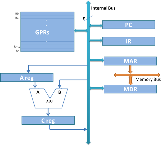
Memory – Instruction memory is mostly read-only in the fetch phase. Data memory is required to access the operand and result writing. The memory is accessed over a bus from the CPU. To access memory, the address of the memory location is required in addition to Read/Write of data. The Memory Address Register (MAR) holds the address of the memory location to be accessed. The Memory Data Register (MDR) holds the data. It holds the data read from memory (Data-in) in the case of memory read; holds the data to be written into the memory location in the case of Memory write operations. Thus MDR is a bidirectional register.
Registers – Registers are in physical proximity and internal to the CPU. These are ultra-fast than Memory. Most of the times the operands are brought from memory and kept in registers. Rather these registers are used as a workspace and rough space for workout.
Register files – These are multiport register set enabling faster and parallel access to the register set.
Internal Registers – Instruction Register, Memory Address Register, Memory Data Register. These are not accessible to the programmer.
Multiplexers – Anything is reachable with these. These allow what is to be allowed out based on the selection input.
Internal bus – which connects all these elements.
Control unit – the master which manages the datapath elements.
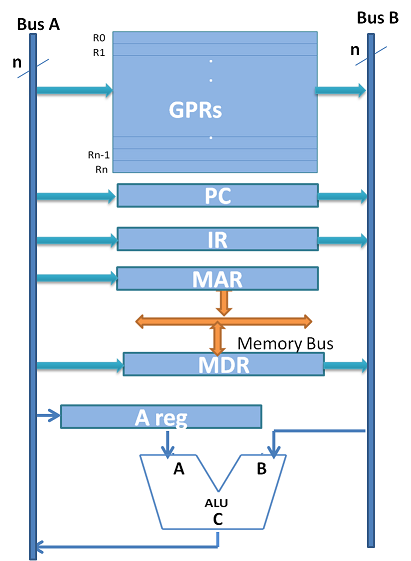
These units are required to be interconnected and work synchronously. Figure 12.1 and 12.2 are two typical datapaths configured wth single bus and two buses respectively. The word BUS is used to mean the career of information and is a physical type, logically controlled for the information that it carries. The bus can carry data in either direction and the data on the bus is valid for the period and the purpose that is controlled by the Control Unit. There are two buses in consideration here. One is an internal bus, whose purpose is to reach data within the CPU. The memory bus, which is external to the CPU. The datapath has A register, an internal register which is required to hold one of the operands for the ALU. In the case single bus datapath, C register, another internal register is required to hold the output of ALU until it is stored in the permanent location. For simplicity, the control unit details are not shown here and will be dealt with in the next chapter. Let us understand the navigation of data with few examples.


Datapath Functioning
Example 1. Instruction Fetch. The table below details, the navigation of information for instruction fetch from memory in the case of Single bus and Two bus datapaths.
| Single Bus operation | Two bus Operation |
|---|---|
| PC holds the instruction to be fetched | PC holds the instruction to be fetched |
| PC -> MAR via internal bus | PC value goes into B Bus; from B Bus via ALU B-side, reaches A-bus and gets clocked into MAR. PC-> B-bus->ALUB side->A-Bus->MAR |
| Memory read initiated in the memory bus | Memory read initiated in the memory bus |
| Data from memory (Instruction in this case) is clocked into MDR | Data from memory (Instruction in this case) is clocked into MDR |
| The instruction in MDR->Instruction register via internal bus | The instruction in MDR->Instruction register via B-bus, ALU, A-bus MDR-> B-bus->ALUB side->A-Bus->IR |
| PC+n ->PC. This step may use a counter associated with PC | PC +n ->PC; This step may use a counter associated with PC. |
Example 2 Store instruction. ST R4, LOC1. The operation to be carried out is the content of Register 4 of GPR to be stored in memory location LOC1. Instruction is decoded in the fetch phase as ST (Store) and the memory location addressLOC1 for storing is available in IR
| Single Bus operation | Two bus Operation |
|---|---|
| IR (ads) -> MAR. There exists a direct path to MAR | IR-> B-bus->ALUB side->A-Bus->MAR |
| Read R4; [R4] -> MDR over the internal bus | Read R4; [R4] is available on B-bus. From B-bus, B=C operation of ALU reaches A-bus and gets clocked into MDR. [R4]-> B-bus->ALUB side->A-Bus->MDR |
| Initiate memory write; i.e Enable MAR on memory bus; enable MDR on memory bus; issue Write signal to Memory | Initiate memory write; i.e Enable MAR on memory bus; enable MDR on memory bus; issue Write signal to Memory |
The data from B-bus is made available at A-bus happens with very little latency. At this time, the reader may not be able to appreciate the benefit of two bus datapath over the simple one bus datapath. However, this will be clarified in the next chapter while dealing with timings. Here we have dealt at the conceptual level.
Three bus and more architecture datapaths are available in later CPUs. These may be studied on a case basis by the reader.

