The purpose of the Control Unit is to generate control signals. These control signals facilitate flawless execution of instructions in CPU, handling of Interrupts and internal errors by CPU, communication over the internal bus(es) in CPU, communication over the external bus (external Datapath) to memory and IO subsystem. A Control unit is part of the CPU subsystem.
Instruction execution is facilitated by a sequence of macro and micro-operations (steps) by the control unit. The number such micro-operations required to complete an instruction depends on the instruction and the datapath. Please recall the topic "Datapath Functioning" in chapter 12, wherein we had seen two examples demonstrating the micro-operations involved in instruction fetch and store operations.
A program consists of a set of instructions. Each instruction is executed with macro steps typically FETCH, DECODE, EXECUTE and RESULT WRITING. The number of such macro steps varies with different CPU design. In some cases of Instruction, Interrupt recognition is an additional machine cycle. Also, Instruction Fetch and Operand Fetch are considered as two different macro steps. These macro steps are also called Machine Cycles. Each of these macro steps has many sub operational steps called micro-operations. The micro-operations are the functional or atomic operations of a Processor. Each micro-operation is executed in one timing state. The period of these timing states corresponds to one CPU clock cycle or multiple clock cycles. Figure 13.1 explains the correlation from program to timing states during the execution flow.

Issues to be considered in the design of Control Unit
The datapath design precedes the Control Unit design. Designing datapath gives a good idea of what control signals are needed.
- Define basic elements of the processor (Datapath elements)
- Describe micro-operations processor performs (how the Datapath can best be used)
- Determine functions the control unit must perform (the Control signals required at timing states)
The micro-operations to be performed by the processor can generally be classified as:
- Data transfer between registers (Ex: ADD R4, R5)
- Data transfer from Register to external subsystems like Memory or I/O (Ex: Store R4, LOC1, OUT #276)
- Data transfer from the external subsystems to Register (Load R4, LOC1, OUT #275)
- Perform arithmetic or logical operations (ALU Operations part of any instruction)
Based on the above datapath and the micro-steps, as above, the functions to be performed by the control unit are identified. The appropriate control signals ensure that the data moves through the datapath in the right way during instruction execution. Generally, one needs to know what the datapath is currently doing, to tell it, what to do next.
The functioning of the Control Unit
We have mentioned that the control unit is in charge of coordinating and synchronizing activities inside the CPU and also with the other subsystems of the computer. A set of control signals activates the micro-operations which have to be executed in a given control step. Each control step corresponds to one clock cycle of the CPU.
Thus the control unit performs two tasks:
- Sequencing - Causing the CPU to step through a series of micro-operations
- Execution - Causing the performance of each micro-op.
The Control Unit is a state machine that generates control signals based on certain inputs. The output signals are generated based on the input conditions to the state machine.
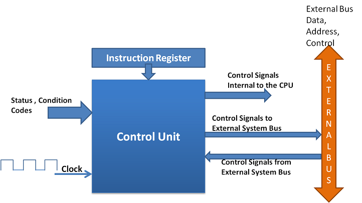
Processor Clock - The clock drives the Control unit and synchronizes the micro-operations. The control unit issues one or more micro-operations per clock cycle. More micro-operations per clock is feasible in a control step subject to (a) the pipelining and parallelism in the architecture and (b) that the micro-operations don’t conflict (for example, only one of them is allowed to output on the bus) with resource usage in that control step.
Instruction register (IR) – IR holds the Op-code for current instruction and plays a major role in the definition of the micro-instructions required. The signals to be generated are written by the designer based on Instruction and the Datapath structure.
Flags and Condition Codes - There are status flags like Trap, Interrupt, Parity, etc along with Condition Codes in the Processor Status register. These indicate the state of CPU and Condition Codes (ZSOC) indicate the results of the previous operations within the CPU.
External Control bus - The external sub-system status is communicated to the CPU over the Control Bus. Signals like Interrupts from IO Subsystem indicate the attention required from CPU. During Memory Read, the memory is required to indicate that Read Data is available on the Data Bus. This is a kind of acknowledgement or sync from memory on the external control bus. Similarly, Interrupt Acknowledgement (IACK) is issued by CPU to the subsystem that has raised the Interrupt as part of the service routine. There are few other signals like these.
Figure 13.2 pictorially represents a model control unit with inputs and outputs.

Outputs from Control Unit
The signals generated at a certain moment depend on:
- the actual step to be executed as defined by the designer based on the datapath and functional units;
- the condition and status flags of the processor;
- the actual instruction being executed ( available in the IR)
- external signals received on the system bus (e.g. interrupt signals).
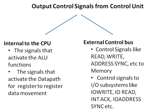
As seen from figure 13.2, the control unit generates signals to facilitate the execution internal to the CPU and also the external subsystems via the external bus.

We have been discussing control signals and the categories that they fall into. Let us see some example cases to get an idea of those signals. Please recall the number of micro-steps and the signal required is CPU implementation-specific. The discussion below is a typical case using single bus datapath intended to create good understanding and kindle imagination.
Example 1: Fetch Machine Cycle
In Chapter12, we had discussed the steps to carried out for Single and Two bus datapath. Now we use the Single bus datapath and identify the control signals required as below.
| Micro-operation | Control Signal Required | Control Signal Category |
|---|---|---|
| PC holds the instruction to be fetched PC -> MAR via internal bus | t1: clock MAR | CPU Internal |
| Memory read initiated in the memory bus | t1: ADS ENABLE MREAD -> Control bus | External Bus |
| Data from memory (Instruction in this case) is clocked into MDR | t2: clock MBR | CPU Internal |
| Data from memory (Instruction in this case) is clocked into MDR | t2: clock MBR | CPU Internal |
| The instruction in MDR -> Instruction register via internal bus | t3: clock IR | CPU Internal |
| PC+n -> PC. This step may use a counter associated with PC | t3: Inc PC | CPU Internal |
The Instruction fetch machine cycle requires 3 steps and executed in 3 timing states i.e. 3 CPU clock cycles. Further notice that in t1 and t3, two micro-steps are carried out and hence the control unit generates two signals.
Please bear in mind that the data available on the internal bus or external bus is required to be clocked into the respective register. If not clocked it is not stored in that register. In t1, PC -> MAR via the internal bus. The signal to be generated is "clock MAR". Although data is available on the internal bus, since “"clock MAR" is the active signal, only MAR stores the value on the internal bus and none other registers on the bus. Similarly, in t3, only IR stores the value on the internal bus and none other. PC, as the name suggests is a counter, and hence increments the value standalone based on the INC PC signal.
Example 2: Store Instruction ST R4, LOC1
Instruction is fetched as above. Decode is a simple demultiplexer or combinational logic operation. Hence let us presume that the instruction is decoded to be store. LOC1 Is the memory location where contents of R4 to be stored. The instruction uses direct addressing and hence LOC1 value is available in IR at the end of Instruction fetch cycle. With this info, let us use the table below to understand the micro-operations in the execute-machine cycle and the signals required.
Execute-machine cycle for STORE operation
| Micro-operation | Control Signal Required | Control Signal Category | |||||||||||
|---|---|---|---|---|---|---|---|---|---|---|---|---|---|
| IR (ads) -> MAR; via internal bus |
| CPU Internal | |||||||||||
| Read R4 |
| CPU Internal | |||||||||||
|
| External Bus | |||||||||||
Example 3: Add instruction ADD R4, LOC1 i.e. [LOC1] +[R4] -> R4; LOC1 =1200, R4=300
| Micro-operation | Control Signal Required | Control Signal Category | |||||||||
|---|---|---|---|---|---|---|---|---|---|---|---|
| IR (ads) LOC1 -> MAR; via internal bus |
| CPU Internal | |||||||||
|
| External | |||||||||
|
| CPU Internal | |||||||||
|
| CPU Internal | |||||||||
|
| CPU Internal |
We have dealt the examples using Single bus datapath. When the CPU has more number of internal buses, then it is likely that the number of timing states required for the machine cycles could be less in a large number of cases. The designer's diligence is highly appreciated as he has to prepare all the list of control signals required for each of the instructions in ISA, interrupt servicing, trap handling, error handling, flags handling etc. The designer writes in Hardware definition language and verifies using the emulator. The logic designer implements the necessary hardware for the control unit.
Intentionally I have avoided timing state diagrams as it will be appreciated only by a select section of readers with Electronics or design background. However, the tables with details of operations in timing state should suffice to give a clear understanding of the Control Unit.

